
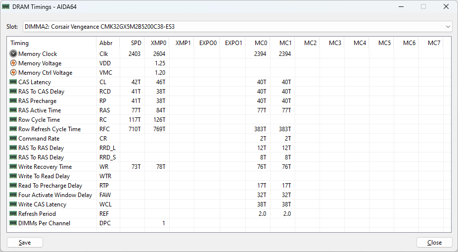
This window provides extremely detailed DRAM timing information, much more than what is available on the Motherboard / SPD page.
Detailed Information for Professional Users
The DRAM Timings window in AIDA64 offers in-depth insights into the various timing parameters of your memory modules. This is crucial for enthusiasts and professionals who need to fine-tune their system for optimal performance or stability. Here is a breakdown of the information and features available:
- Memory Clock (Clk): Displays the operating frequency of the memory module. This is the speed at which the memory operates and is a critical parameter for performance tuning.
- Memory Voltage (VDD): Indicates the voltage supplied to the memory module. Proper voltage settings are essential for stability, especially when overclocking.
- Memory Ctrl Voltage (VMC): Shows the voltage of the memory controller. Adjusting this can help stabilize the memory when running at higher frequencies.
- CAS Latency (CL): The delay between the READ command and the moment data is available. Lower values can improve performance but may require higher voltage or better quality memory modules.
- RAS to CAS Delay (RCD): The delay between the RAS (Row Address Strobe) and CAS (Column Address Strobe) signals. Fine-tuning this can improve data throughput.
- RAS Precharge (RP): The time needed to precharge the row access. This timing affects the memory’s ability to quickly switch between different rows of data.
- RAS Active Time (tRAS): The time a row remains active before precharging. Balancing this with other timings can impact overall memory performance.
- Row Cycle Time (tRC): The total time for a row to cycle, combining active and precharge times.
- Row Refresh Cycle Time (tRFC): The time needed to refresh a row. Critical for memory stability, especially in high-density modules.
- Command Rate (CR): The delay between when a memory chip is selected and when the first active command can be issued. A 1T command rate offers better performance but may be less stable than 2T.
- RAS to RAS Delay (RRD): The minimum time between two consecutive RAS commands. This can influence how quickly the memory can switch between different banks.
- Write Recovery Time (WR): The delay after a WRITE command before a PRECHARGE command can be issued. Ensures data integrity during write operations.
- Write to Read Delay (WTR): The delay between a write and a subsequent read command. Optimizing this can improve read-write efficiency.
- Read to Precharge Delay (RTP): The delay from a read command to a precharge command. Affects the ability to quickly switch to different operations.
- Four Activate Window Delay (FAW): The time window in which four active commands can be issued. Important for controlling power and performance balance.
- Write CAS Latency (WCL): Specific latency for write operations. Adjusting this can fine-tune write performance.
- Refresh Period (REF): Indicates the frequency of memory refresh operations. Essential for maintaining data integrity over time.
- DIMMs Per Channel (DPC): Displays the number of DIMMs installed per memory channel, affecting overall memory bandwidth and latency.
Available in the following products:
AIDA64 Business
AIDA64 Engineer